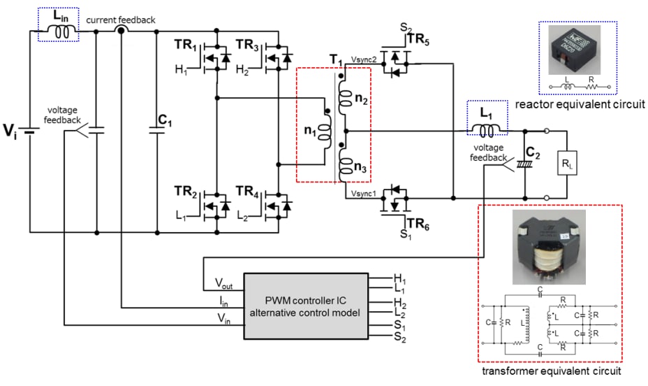
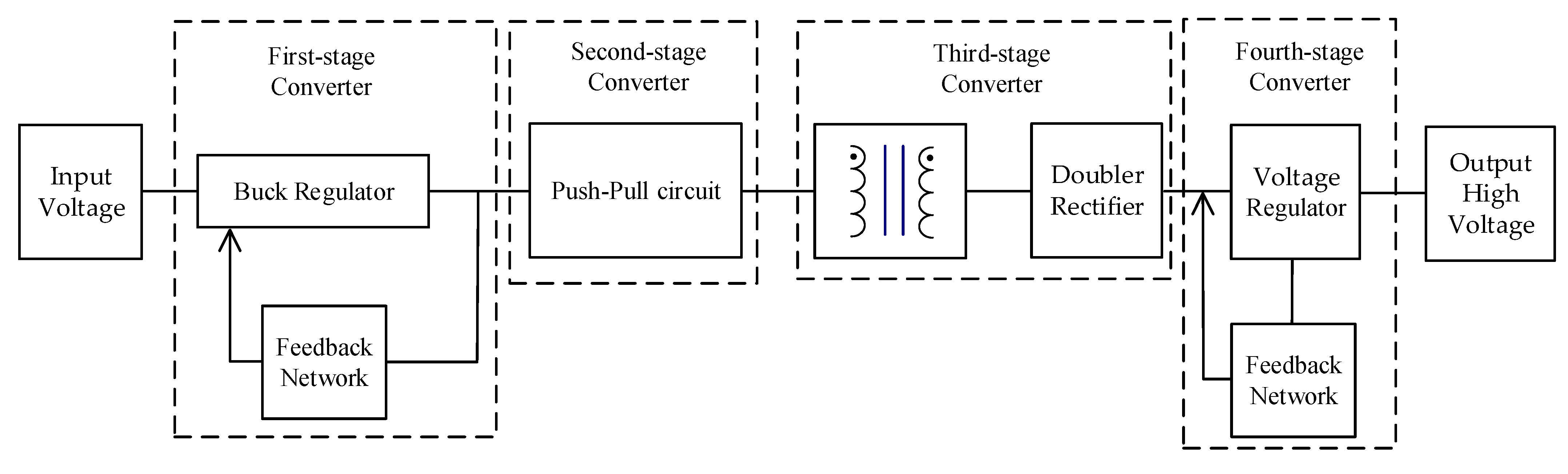
Design for a FourStage DCDC HighVoltage Circuit Diagram
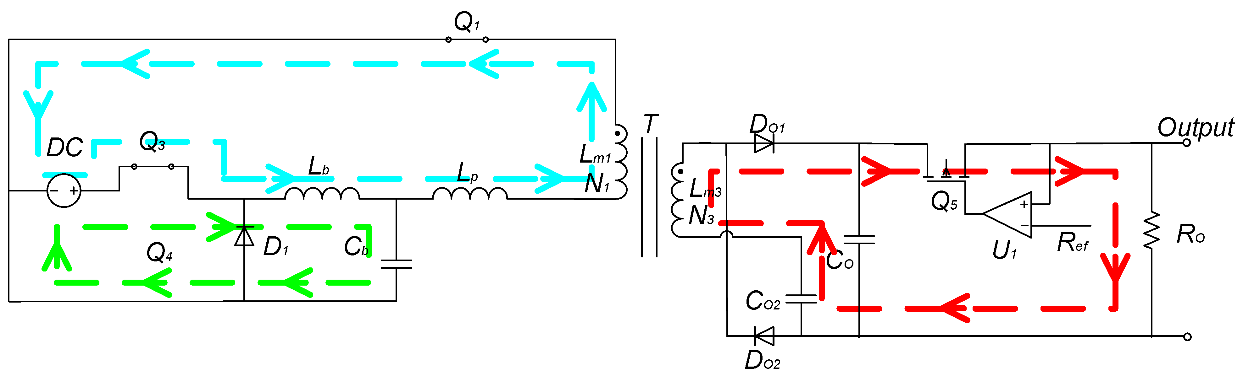
Design for a FourStage DCDC HighVoltage Circuit Diagram The 5kW Isolated Bidirectional DC -DC Converter reference design from Toshiba shows how to improve a power supply design's efficiency using SiC MOSFETs. The design uses the dual active bridge (DAB) method, one of the most popular topologies for such high-power converters. The DAB topology has full bridges on both sides, allowing the direction and
Designing a high efficiency DC-DC converter for these portable devices is challenging due to the special requirements of a battery operated system, such as a wide input voltage variation and dynamic operating load. The following sections, present the fundamentals and design considerations of various portable DC-DC Introduction. A DC-DC converter is an essential component in modern electronics, used to step up or step-down voltage efficiently. High-efficiency designs are crucial in power-sensitive applications such as renewable energy systems, electric vehicles, industrial power supplies, and IoT devices.. This guide provides a step-by-step approach to designing a high-efficiency DC-DC converter Like a linear regulator, the DC-DC converter can regulate to a lower voltage. Unlike linear regulators, however, the DC-DC converter can boost an input voltage or invert it to create a negative voltage. As an added bonus, the DC-DC converter boasts efficiencies greater than 95% under optimum conditions.
Calculating Efficiency (Rev. A) Circuit Diagram
Efficiency in a DC-DC Converter. There are many sources of loss in a DC-DC converter that reduce the efficiency of the system. These losses can be divided into two basic groups: efficiency losses caused by peak inductor current; and switching losses that occur each time that the circuit switches from charging to discharging phases.
The three-level buck converter in figure 3 was built to verify the design. The overall thickness of the circuit including the circuit board is only 5 mm. The circuit was tested with no forced air up to 12.5 A output current with a temperature rise of 65 °C. The switch-node voltage V SW waveform at 8 A output current is shown in figure 4.
How to Design High Circuit Diagram
This is particularly helpful in high-frequency, high-conversion ratio applications, because it allows for more precise control and minimizes the effect of delays due to other circuit elements. 2.